- Shenzhen Chaosheng Electronic Technology Co., Ltd.
-
 1YrShenzhen, Guangdong, China
 - Main products: Oversized PCB, Any order HDIPCB, High frequency hybrid HDIPCB, Special material PCB
Home > Products > Multi layer flexible FPC > 10L flexible FPC second stage
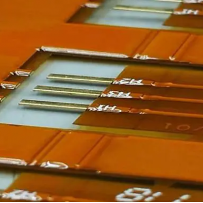


10L flexible FPC second stage
- Shenzhen Bay, Guangdong, China
- T/T
- 20 days
You May Like
-
 10 layer third-order HDI flexible FPC
-
Fake double-layer floor hollow FPC, pure copper based floor hole FPCÕQīMulti layer flexible FPC
-
Transparent FR-4PCB,FR-4, TG130 materialÕQīPI transparent flexible board FPC
-
1.60mm transparent FR-4PCBÕQīUltra thin transparent FR-4PCB
-
blind buried hole HDI flexible FPC,4-layer flexible FPC
-
12 layers of flexible multi-layer,soft hard combined FPC,Mobile phone motherboard, touch screen
Product Details
| Material | Polyester Film | Application | Digital Products, Computer with LCD Screen, Mobile Phone, Aviation and Aerospace | |
| Structure | Double-Sided FPC | Brand | China Chaosheng FPC | |
| Flame Retardant Properties | V0 | Insulation Materials | Metal Composite Materials | |
| Processing Technology | Electrolytic Foil | Combination Mode | Without Adhesive Flexible Plate | |
| Conductive Adhesive | Conductive Silver Paste | Base Material | Aluminum | |
| Transport Package | Vacuum packaging+separated white paper+moisture-proof beads+wooden pad | Specification | 56*68mm | |
| Trademark | no | Origin | China,Guangdong,Shenzhen |
Product Description
Product field: Automobile battery products
Number of layers: 10L flexible FPC second order
Plate thickness: 0.350mm
Size: 142 * 106.0mm/1 * 1 piece
Process structure: PI, copper thickness 1OZ, covering film
The minimum mechanical hole is 0.35mm.
Laser hole 0.076mm
Minimum line width and spacing 5/5ml
Surface treatment: 1u of gold"
| Main Product Structure of Chaosheng Group Company 2-80 layers of rigid circuit boards, 2-50 layers of flexible circuit boards and PCBA production Chaosheng Group Company mainly produces product categories High end double-sided, multi-layer, flexible, high-frequency, HDI interconnect, metal based, high thermal conductivity metal based, ceramic, cut in metal based, cut in buried capacitor, cut in thick copper buried magnet, concave convex step substrate, 5G high-speed board, thick copper, thick gold, high carbon resistance, double-sided multi-layer MiNiLED, MiNiHDILED, MiNiOLED, IC carrier substrate, roll to roll FPC, long FPC, large-sized printed circuit board, halogen-free material, high-frequency material, high-speed material, metal material, environmentally friendly circuit board, blind buried hole circuit board, high thermal conductivity aluminum based, thermoelectric separation copper based, PDU busbar, iron-based and metal based (core) mixed pressure plate, embedded copper buried copper.Buried resistance buried capacitance buried ceramic bead board, ultra-thin BT board, ceramic substrate, IC carrier board, high-frequency mixed voltage, high-speed board, differential impedance board, thick copper plate, thick gold plated board, HDI An integrated OEM and ODM production factory for Anylayer, double-sided, multi-layer, HDI FPC, soft hard combination HDI, roll to roll FPC, ultra long FPC, ultra large size PCB production and product design and development, software development, special material printed circuit boards, etc.roll to roll FPC, ultra long FPC, ultra large size PCB production and product design and development, software development, special material printed circuit boards, etc.roll to roll FPC, ultra long FPC, ultra large size PCB production and product design and development, software development, special material printed circuit boards, etc. The main application areas of PCB and PCBA products of Chaosheng Group Company Communication terminals, communication stations, electronic communication, fiber optics, optical modules, backlight sources, chip systems, communication equipment, communication instruments, computers, intelligent devices, intelligent control, system control, industrial power control, industrial equipment, testing instruments, testing instruments, SD cards, SG cards, mobile phones, computers, various antennas, radars, automobiles, light sources, resistors, music equipment, playback equipment, banking equipment, medical instruments, medical equipment, aerospace, aviation, military, LED, OLED, OLCD power control power supply, industrial power supply, communication power supply, automotive power supply, office equipment, digital products, computers and other application fields; The main application areas of flexible circuit boards (FPC) and FPCA products of Chaosheng Group Company Hard drives, printers, fax machines, scanners, sensors, mobile phones, connectors, modules, walkie talkie antenna cards, high-end cameras, digital cameras, laser heads, CDs, medical devices, instruments, drives, automobiles, automotive instruments, automotive drive disks, drivers, optical drives, medical devices, medical equipment, backlight sources, modules, banking equipment, industrial instruments, LED light strips, military, aviation, aerospace, national defense and other product fields. | |||||||||||||||
| Serial Number | Project | Manufacturing capability | |||||||||||||
| 1 | Layers | Floors 1-80 | |||||||||||||
| 2 | Maximum size of PCB | 2500*1150mm | |||||||||||||
| 3 | Maximum size of flexible FPC | 500mm*100m | |||||||||||||
| 4 | Maximum size of PCBA | 1600mm*1000mm | |||||||||||||
| 5 | FPCBA maximum size | 500mm*100m | |||||||||||||
| 6 | PCB finished product thickness | 0.15-12.0mm | |||||||||||||
| 7 | Thickness of flexible FPC finished product | 0.05-0.60mm | |||||||||||||
| 8 | Finished copper thickness | 12um-1075um | |||||||||||||
| 9 | Minimum finished aperture of laser hole | 0.075mm | |||||||||||||
| 10 | Minimum line width and spacing | 1.5mi/1.50mil | |||||||||||||
| 11 | Minimum finished hole diameter for through-hole | 0.15mm | |||||||||||||
| 12 | Thickness stacking aspect ratio | 1:35 | |||||||||||||
| 13 | By processing methods | VIA blind buried hole treatment: ink plug hole, resin plug hole, copper paste plug hole, VCP copper filling hole, silver paste plug hole, carbon oil plug hole, etc | |||||||||||||
| 14 | Surface Treatment | Sinking gold, electroplating nickel gold, electroplating thick gold, electroplating gold+OSP, electroplating nickel gold+sinking gold, electroplating nickel gold+sinking gold+OSP, electroplating gold+OSP, electroplating gold+gold fingers, OSP+gold fingers, lead-free tin spraying, lead-free tin spraying+sinking gold, lead-free tin spraying+gold fingers, lead tin spraying, OSP, sinking tin, sinking silver, electroplating silver | |||||||||||||
| 15 | Main substrate brands | Rogers, Arlon, Taconic, TP-2, Megtron, Neclo, Isola, F4B, 3M, Mitsui Group (Japan Mitsui/Mitsui Top), Taiyo TUC, Taiguang EMC, Tenghui VT, Shengyi SY, Lianmao ITEQ, South Asia NOUYA, DuPont Kappon, Taihong, Hongren Hongren, Xin Yang, Nippon Steel Nippon Stee, Teflon, Yasen, Matsushita, RCC, Mitsui Mitsui Group (Japan Mitsui Top), 3M (USA) 3M Location, Kyocera CERADIR, Jiuhe, Jiuhao, China Porcelain, Huaqing, Ai Shengda, Slitton, Kai Changde, Tongxin, Bergs, Yalong, Taiconieta, etc | |||||||||||||
| 16 | Solder mask color | Green, black, red, yellow, white, blue, purple, matte green, matte black, etc | |||||||||||||
| 17 | Test service | AOIŃĆüX-RayŃĆ?Voltage withstand test, short circuit test, soldering test, thermal shock test, functional test, high temperature and high humidity test, first piece tester, etc | |||||||||||||
| 18 | Molding method | CNC shape, punch shape, V-CUT+forming method | |||||||||||||
| 19 | Finished product warpage | Ōē?.5% | |||||||||||||
| 20 | Mechanical aperture tolerance | Ōē?.025mm | |||||||||||||
| 21 | Finished product warpage | Ōē?.5% | |||||||||||||
| 22 | MiNiLED Minimum PAD | 0.065mm/0.065mm | |||||||||||||
| 23 | Thermal conductivity | Ōē?W | |||||||||||||
| 24 | Highest withstand voltage | 2500Pa | |||||||||||||
| 25 | High carbon resistance value and tolerance | Ōē?00Ōå?5000╬®¹u20% | |||||||||||||
| 26 | Impedance tolerance | Ōē? Ōå?8%Žē | |||||||||||||
| 27 | IC Carrier Board Series | Minimum line width and spacing of 20um/20um | |||||||||||||
| FAQ | |||||||||||||||
| Question Point | Answer | ||||||||||||||
| Q: What information is required for PCB | CEGSATE: Gberber files for PCB production, product process instructions, such as material requirements, surface treatment requirements, finished product thickness requirements, PCB stack structure diagram for advanced products, copper thickness requirements for each layer, sample quantity requirements, batch order requirements, product application fields, and other related information are required | ||||||||||||||
| Q: What information does PCBA need to provide | CEGSATE: BOM report is required (including the brand, specifications, and model of the components), X and Y coordinate numbers of PCBA components, and processing requirements: Do we need to purchase the components on our behalf? Or customer supplied components? Do you need software burning? What is the required quantity? What is the monthly demand and other detailed information. | ||||||||||||||
| Question: Is my file secure? | CEGSATE: Your files are very secure, and we protect intellectual property rights for our clients throughout the entire process. All files provided by the customer will never be shared with any third party. | ||||||||||||||
| Q: What is the minimum order quantity? | CESGATE: There is no minimum order quantity in POE. We are able to handle small and large batches flexibly. | ||||||||||||||
| Q: Do you have any other services? | CESGATE: We mainly focus on PCB+FPC production+SMT+assembly PCBA+component procurement services; In addition, we can also provide programming, testing, software burning, wiring, and shell assembly services; And product design, product development, software development | ||||||||||||||
| Q: What is your inspection method? How do you control the quality? | CESGATE: In order to ensure the quality of PCB and FPC products, flying pin testing is usually used for samples and small batches; The inner circuit undergoes AOI optical inspection, online AOI inspection, and the finished product undergoes 100% inspection through E-SET testing rack. The appearance undergoes 100% inspection through fully automatic finished product inspection equipment and FQC. PCBA undergoes automatic optical inspection (AOI), BGA part X-Ray 100% radiographic inspection, and first article inspection (FAI). PCBA products that require software burning undergo 100% full testing through finished product testing rack according to product functional requirements. | ||||||||||||||
Company Profile
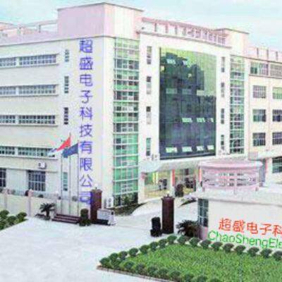
Company Profile The development history of Chaosheng Group shows a typical trajectory from its establishment to growth into a leader in the printed circuit board industry. A brief overview of Chaosheng Group, its subsidiaries, and specialty products: History and Background of Chaosheng Company: Chaosheng Group was founded in 1968, originating from Japan, under the name Chaosheng Technology Japan Kawasaki Co., Ltd. In 2012, the company implemented a shareholding reform, marking a shift towards more modern and standardized management. As a Sino Japanese Hong Kong joint venture, Chaosheng Group holds an important position in the Chinese circuit board manufacturing industry. Global factory distribution Zhejiang Kunying Electronic Technology Co., Ltd. (formerly renamed after the merger of Taiwan Kunying Electronics) was established in 2001, increasing the production and technical capabilities of Chaosheng Group in the field of circuit boards. Mainly focusing on high-end precision flexible circuit boards. Shenzhen Chaosheng Electronic Technology Co., Ltd. and Shenzhen Guangrui New Electronics Co., Ltd. (formerly known as Shenzhen Mingze Electronics Co., Ltd.) were established in 1993 and 2008 respectively, further expanding Chaosheng Group's layout in the Chinese market. We mainly provide supporting processing factories for customers in product design, software development, product research and development, and SMT surface mount processing. Chaosheng Group has multiple sales networks worldwide, covering France, the United Kingdom, Germany, Japan, Europe, Switzerland, Africa, North America, Austria, Taiwan, Hong Kong and other countries and regions, showcasing its global influence. Product Features and Applications: Widely used products: communication equipment, communication instruments, optical communication, infinite terminals, new energy, intelligent systems, medical devices, detection systems, aviation, aerospace, military, drones, robots, AI technology, 5G equipment, 5G communication, optical products, LEDŃĆ?The high-tech fields such as communication, automotive, and home electronics reflect the technological strength and market insight of Chaosheng Group. Main materials: halogen-free materials FR-4ÕQ?Polyimide PI materials, high TG materials, high-frequency materials, high-speed materials, metal materials, glass materials, embedded materials, transparent FR-4 materials, heat dissipation materials, embedded materials, high thermal conductivity metals, high thermal conductivity aluminum substrates, environmentally friendly circuit boards, BT materials, ABF materials, etc. Product structure: Metal based mixed pressure plate, embedded copper, buried resistance, buried capacitance, buried ceramic bead plate, buried ceramic, ceramic mixed pressure, multi-layer ceramic, BT board, ultra thick PCB, multi-layer aluminum substrate, high-frequency mixed pressure, impedance board, thick copper plate, thick gold plated board, high and low copper, high carbon resistance, transparent FR-4 multi-layer, glass plate AnylayerŃĆ?Single, double, multi-layer, soft and hard combination HDI, roll to roll FPC, ultra long and ultra large size boards, PCB production and product design and development, software development and SMT, PCBA and other integrated production factories The annual output value of Chaosheng Group exceeds 100 billion yuan, with the annual output value of printed circuit boards reaching over 65 billion yuan, demonstrating its strong production capacity and market competitiveness. With the continuous advancement of technology and changes in the market, Chaosheng Group needs to continue to pay attention to the dynamics of new technologies, products, and markets, strengthen research and development investment and innovation capabilities, in order to maintain its competitive advantage and industry position.
Contact Us
- Shenzhen Chaosheng Electronic Technology Co., Ltd.
- Contact nameMank.Li Chat Now
- Phone86-0755-89586738
- AddressAilian community shigangxu rd industrial zone, Shenzhen, Guangdong
Product Categories
New Products
-
Aviation Bluetooth GlassesÕQ?6 layers HDI 4th order
-
PET transparent single-layer double-layer flexible FPC,Single layer PET material flexible flexible board FPC
-
Apple iPhone 12 layer arbitrary soft hard combination HDIFPC
-
iPhone 12 layer arbitrary soft hard combination HDI Flexible FPC,multi-layer flexible HDIFPC,
-
6L high-speed rail car high-voltage soft hard combination FPC
-
2-layer SG card, SD card, thick goldPCBÕQīMulti layer ultra-thin PCB
-
2-layer thin plate thick gold PCB,Ultra thin thick gold SG card gold finger PCB
-
2-layer ultra-thin ultra large size PCB,Ultra thin multi-layer PCB
-
2-layer thin plate+thick metal+high carbon resistancePCB,Micro motor ultra-thin high carbon resistance PCB
-
4-layer 15OZ thick copper+copper bar+copper based charging pile PCB,High thermal conductivity copper based+8W adhesive PCB
-
4-layer high-voltage thermoelectric separation thick copper aluminum substrate
-
2layer high-voltage thermoelectric separation thick copper aluminum substratePCB
-
2-layer thermoelectric separation high current multi-layer aluminum based PCB
-
4 thick copper high thermal conductivity thermoelectric separation aluminum basePCB
-
4-layer thermoelectric separation high current multi-layer aluminum based PCB,Thermoelectric separation aluminum based circuit board PCB
-
6layers of copper with a thickness of 210um, thermoelectric separation aluminum basedPCB
-
4-layer recessed thick copper charging pile PCB,Bent copper electrolytic PCB
-
Bend type recessed copper based PCB,Inward bending copper based PCB
-
Inlaid thick copper bent PCB,Bent copper electrolytic PCB
-
False 2-layer recessed thick copper bent PCB
-
2-layer false double-layer recessed thick copper bent PCB,Inward bending copper based PCB
-
12 layers, 2nd order high-frequency mixed voltage, 2nd step PCB
-
16 layers, 3rd order high-frequency mixed voltage, 6 step PCB
-
8 layers, 3rd order HDI high-frequency mixed pressure buried copper PCB,8th layer 3rd order optical module buried resistance PCB
Popular Searches
- Flexible Pcb
- fpc
- mobile pcb
- flex-pcb
- Flexible Printed Circuit Board
- flex cable fpc
- Pcb Assembly Fpc
- Flex Cable Pcb
- Rigid Flex Pcb
- Fpc Circuit Board
- mobile phone pcb board
- phone pcb
- flex pcb
- fpcb
- single sided pcb board
- Mobile Phone Pcb
- conductive
- customized fpc
- copper fpc
- flexible circuit board
- Circuit Board Fpc Cable
- Flex Pcb Cable
- Rigid Flex Pcb Board
- flexible printed circuits
- Flex Circuit Board
- Electronic Products Pcb
- flex pcb assembly
- Flex Pcb Board
- fpc connect
- lcd pcb
Find Similar Products By Category
- Electrical & Electronics > Circuit Board > FPC
Shenzhen Chaosheng Electronic Technology Co., Ltd.

- Please Enter your Email Address
- Please enter the content for your inquiry.
We will find the most reliable suppliers for you according to your description.
Send Now-
 Mank.Li
Hi there! Welcome to my shop. Let me know if you have any questions.
Mank.Li
Hi there! Welcome to my shop. Let me know if you have any questions.
Your message has exceeded the limit.
- Contact supplier for lowest price
- Customized Request
- Request Sample
- Request Free Catalogs
Your message has exceeded the limit.
-
Purchase Quantity
-
*Sourcing Details
Your inquiry content must be between 10 to 5000 characters.
-
*Email
Please enter Your valid email address.
-
Mobile
We will contact you as soon as possibleÕQ?/p> Continue View